News BoT
RSS Feed
Joined: 11 May 2006
Posts: 32637
 |
 Posted: Fri Jun 01, 2012 8:00 am Post subject: The Rest of the Ivy Bridge Die Sizes Posted: Fri Jun 01, 2012 8:00 am Post subject: The Rest of the Ivy Bridge Die Sizes |
  |
|
<p align="center"> </p><p><p> </p><p><p>
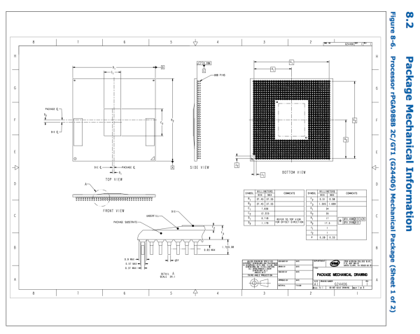
AnandTech reader <strong>Grant Vezina</strong> pointed out in the comments to my last post that Intel properly documents almost all Ivy Bridge die sizes in the mechanical specifications pages of its Ivy Bridge datasheets. That's what I get for feeling accomplished after taking apart the Zenbook Prime and measuring its Core i7-3517U. Only the 4C/GT2, 2C/GT2 and 2C/GT1 dimensions are documented while the 4C/GT1 configuration is <strong>Vezina's</strong> own calculation based on available data. </p>
<table align="center" border="0" cellpadding="0" cellspacing="1" width="575">
<tbody>
<tr class="tgrey">
<td align="center" colspan="10">
Ivy Bridge Die Comparison</td>
</tr>
<tr class="tlblue">
<td width="120">
CPU</td>
<td align="center" valign="middle" width="85">
CPU Cores</td>
<td align="center" valign="middle" width="85">
L3 Cache</td>
<td align="center" valign="middle" width="85">
GPU Config</td>
<td align="center" valign="middle" width="85">
Dimensions</td>
<td align="center" valign="middle" width="85">
Die Area</td>
</tr>
<tr>
<td class="tlgrey">
Ivy Bridge HE-4</td>
<td align="center" valign="middle">
4</td>
<td align="center" valign="middle">
8MB</td>
<td align="center" valign="middle">
GT2</td>
<td align="center" valign="middle">
8.141 x 19.361 mm</td>
<td align="center" valign="middle">
159.8mm<sup>2</sup></td>
</tr>
<tr>
<td class="tlgrey">
Ivy Bridge HM-4</td>
<td align="center" valign="middle">
4</td>
<td align="center" valign="middle">
6MB</td>
<td align="center" valign="middle">
GT1</td>
<td align="center" valign="middle">
7.656 x 17.349 mm</td>
<td align="center" valign="middle">
132.8mm<sup>2</sup></td>
</tr>
<tr>
<td class="tlgrey">
Ivy Bridge H-2</td>
<td align="center" valign="middle">
2</td>
<td align="center" valign="middle">
4MB</td>
<td align="center" valign="middle">
GT2</td>
<td align="center" valign="middle">
8.141 x 14.505 mm</td>
<td align="center" valign="middle">
118.1mm<sup>2</sup></td>
</tr>
<tr>
<td class="tlgrey">
Ivy Bridge M-2</td>
<td align="center" valign="middle">
2</td>
<td align="center" valign="middle">
3MB</td>
<td align="center" valign="middle">
GT1</td>
<td align="center" valign="middle">
7.656 x 12.223 mm</td>
<td align="center" valign="middle">
93.6mm<sup>2</sup></td>
</tr>
</tbody>
</table>
<p>
There are a few items of interest here. The GT1 configs appear to be narrower than the GT2 counterparts, otherwise these chips just differ in terms of die length. Haswell will likely continue the trend. </p>
<p>
Why did Intel stop at 16 EUs for the GT2 in Ivy Bridge? Cost is an obvious concern (Intel likes making tons of money) but at some point you need to scale up memory bandwidth to make use of additional compute horsepower. Haswell will address this issue while it scales up to 40 EUs. Intel could have implemented eDRAM with Ivy Bridge, however only one customer was really asking for it and wasn't interested in paying a significant premium for it. Why pay now when Haswell will deliver it less than a year later?</p>
<p>
<div>Gallery: The Rest of the Ivy Bridge Die Sizes<div>     </div></div></p> </div></div></p>
</p>
Read more...
Source: AnandTech
This channel features the latest computer hardware related articles. |
|