News BoT
RSS Feed
Joined: 11 May 2006
Posts: 32637
 |
 Posted: Thu May 23, 2013 8:00 am Post subject: A Closer Look at the Kabini Die Posted: Thu May 23, 2013 8:00 am Post subject: A Closer Look at the Kabini Die |
  |
|
<p align="center">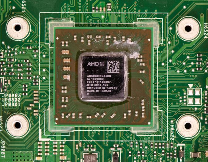 </p><p><p> </p><p><p>
With our review done I did the one thing I've been keeping myself from doing for the past week: I pulled the heatsink off my Kabini review notebook and grabbed a shot of the SoC.</p>
<p>
I guess this is technically the world's first consumer quad-core x86 SoC. Haswell will come in a single-chip solution as well but only as a dual-core part. Kabini needs no companion platform/IO controller chip, everything is integrated on this single piece of silicon. There are also two GCN compute units in there.</p>
<p>
I'm sure AMD will have more accurate numbers shortly, but using my completely unimpressive calipers I measured the die at 10.35mm x 10.35mm (107mm^2). I figure the actual number will be somewhere in the range of 104 - 112mm^2. AMD's 40nm Zacate by comparison (Brazos platform) was a 75mm^2 die, but that's not including the Hudson FCH (Fusion Controller Hub) which was around another 28mm^2. If you add those two up you get roughly the die area of a quad-core Kabini. The beauty of Moore's Law is that although die sizes may be similar, Kabini is appreciably quicker than Zacate.</p>
</p>
Read more...
Source: AnandTech
This channel features the latest computer hardware related articles. |
|

